Debrick Wireless Router Using TUMPA and zJTAG

10 PCS, 10cm x 10cm, 2 layers prototype for $38.80 shipped!
Contents
Buy various JTAG cables for your Satellite Receiver, Cable Modem, Wireless Router, Standard Wiggler from http://www.easymg.com and http://www.diygadget.com
Overview
The TIAO USB Multi Protocol Adapter (TUMPA) is a multi-functional USB communication adapter for hobbyists or engineers. The adapter is based on FDTI's flagship communication chip FT2232H, a USB 2.0 Hi-Speed (480Mb/s) to UART/FIFO IC. It has two multi-protocol synchronous serial engines (MPSSEs) which allow for communication using JTAG, I2C and SPI on two channels simultaneously.
In this tutorial, we are going to show you how to debrick a wireless router. We use WRT54GS as an example, however, it doesn't mean than you can only debrick WRT54GS with TUMPA. You can follow the same instruction to debrick other wireless routers.
Required Hardware and Software
- Obviously, a bricked wireless router (in this example, I am using a bricked Linksys WRT54GS)
- TIAO USB Multi Protocol Adapter (TUMPA)
- Wireless router debrick software [zJTAG]
Disassemble your router
The first step is to disassemble your router. In this example, the WRT54GS is very easy to disassemble. See reference here: Debrick Routers Using JTAG Cable. If you don't know how to disassemble your router, just search it on google :-)
Locate the JTAG Header/Pin on the router's PCB board
The JTAG pin on the WRT54GS is the JP2. See reference here: Debrick Routers Using JTAG Cable
Install TUMPA Drivers
Depending on your system, you can follow the following tutorials to install the drivers on your Windows machine:
How to install TIAO USB Multi Protocol Adapter Driver on Windows XP
How to install TIAO USB Multi Protocol Adapter Driver on Windows Vista or Windows 7
Once the driver is installed, unplug TUMPA from your USB port.
Make The Connections
Once you have identified the JTAG pins on your router, you can connect the router with TUMPA board with the supplied female to female flex cable now. We recommend to use the short cable.
The pinout on the router is as follows:
nTRST  1   2 GND
TDI    3   4 GND
TDO    5   6 GND
TMS    7   8 GND
TCK    9  10 GND
nSRST 11  12 GND
and the pinout one the TUMPA is:
| Pin # | Description |
|---|---|
| 1 | VTAR |
| 3 | nTRST |
| 5 | TDI |
| 7 | TMS |
| 9 | TCK |
| 11 | RTCK |
| 13 | TDO |
| 15 | RST |
| 17 | DBGRQ |
| 19 | DBGACK |
| 2 | Not Connected |
| 4, 6, 8, 10, 12, 14, 16, 18, 20 | GND |
So, it is easy to make the connections: (Make sure both router and TUMPA are not powered on)
Use a flex female to female to connect TDI together (PIN 3 on Router to PIN 5 on TUMPA's 20 PIN JTAG Header
Use a flex female to female to connect TCK together (PIN 9 on Router to PIN 9 on TUMPA's 20 PIN JTAG Header
Use a flex female to female to connect TMS together (PIN 7 on Router to PIN 7 on TUMPA's 20 PIN JTAG Header
Use a flex female to female to connect TDO together (PIN 5 on Router to PIN 13 on TUMPA's 20 PIN JTAG Header
Use a flex female to female to connect GND together (PIN 4 on Router to PIN 4 on TUMPA's 20 PIN JTAG Header
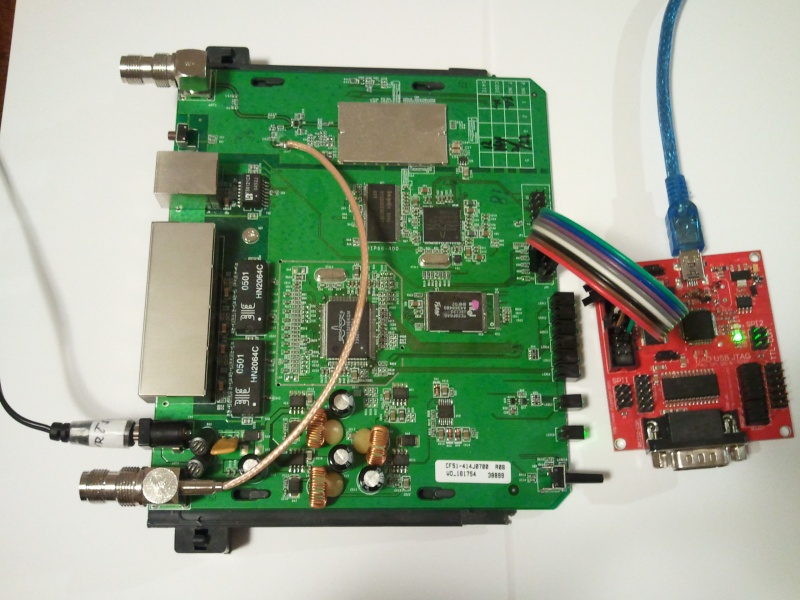
So, it will look like this:
OK, double check the connections, do not power on both router and TUMPA yet.
Get zJTAG Ready
Download zJTAG and unzip it to an empty directory. In my example, I unzipped it to d:\dev\debrick\zJTAG directory.
Double check connections make sure they are correct and secure. Then, connect router to the power outlet and connect TUMPA to your computer's USB port via an USB cable (USB A to Mini B, most digital cameras and camcorders use this kind of cable).
Run zJTAG to Debrick Your Router
It's time to debrick your router now. First, open a DOS prompt window, runzjtagwithout parameters will give you all the command line options.
The following are useful commands:
-probeonly -> Detect router's CPU and Flash chip.
-erase:<area name> -> example: -erase:NVRAM
-backup:<area name> -> example: -backup:CFE
-flash:<area name> -> example: -flash:Kernel
Also, the most important flag is JTAG clock speed divider
/L1:<divider>. TUMPA can clock TCK as high as 30Mhz, however most router's CPU cannot handle such high clock speed, thus you will have to slow down the clock to make it work.
This is the formula:
Speed in KHz = 30000 / (divider + 1)
For example, if you give the following option:
/L1:3
The TCK clock speed is 7500KHz or 7.5MHz (30000/(3+1)).
Let's detect the CPU and Flash now by running the following command:
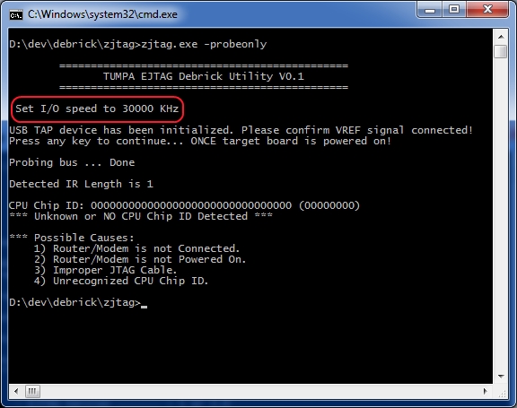
zJTAG -probeonly
As you can see from the above photo, the TCK is set to 30Mhz, however, zJTAG won't be able to detect the CPU and Flash.
Now if we run it with /L1:3 option:
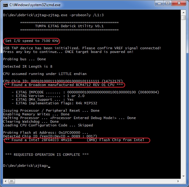
zJTAG -probeonly /L1:3
Once we set the TCK to 7.5Mhz, now zJTAG is able to detect CPU and Flash for my WRT54GS.
Most time, you only need to erase NVRAM, so let's do it:
D:\dev\debrick\zjtag>zjtag.exe -erase:NVRAM /L1:3

        ==============================================
               TUMPA EJTAG Debrick Utility V0.1
        ==============================================


 Set I/O speed to 7500 KHz

USB TAP device has been initialized. Please confirm VREF signal connected!
Press any key to continue... ONCE target board is powered on!

Probing bus ... Done

Detected IR Length is 8

CPU assumed running under LITTLE endian

CPU Chip ID: 00010100011100010010000101111111 (1471217F)
*** Found a Broadcom manufactured BCM4712 REV 01 CPU ***

    - EJTAG IMPCODE ....... : 00000000100000000000100100000100 (00800904)
    - EJTAG Version ....... : 1 or 2.0
    - EJTAG DMA Support ... : Yes
    - EJTAG Implementation flags: R4k MIPS32

Issuing Processor / Peripheral Reset ... Done
Enabling Memory Writes ... Done
Halting Processor ... <Processor Entered Debug Mode!> ... Done
Clearing Watchdog ... Done
Loading CPU Configuration Code ... Skipped

Probing Flash at Address: 0x1FC00000 ...
Detected Chip ID (VenID:DevID = 0089 : 0017)
*** Found a Intel 28F640J3 4Mx16       (8MB) Flash Chip from Intel

    - Flash Chip Window Start .... : 1C000000
    - Flash Chip Window Length ... : 00800000
    - Selected Area Start ........ : 1C7E0000
    - Selected Area Length ....... : 00020000

*** You Selected to Erase the NVRAM.BIN ***

=========================
Erasing Routine Started
=========================
Total Blocks to Erase: 1

Erasing block: 64 (addr = 1C7E0000)...Done
=========================
Erasing Routine Complete
=========================
elapsed time: 3 seconds


 *** REQUESTED OPERATION IS COMPLETE ***


D:\dev\debrick\zjtag>
It's always a good idea to check the result of an erase or flash by running a backup command to compare the output.
In the case of erase, after the action, each bit of the whole area should be 1 (or each byte should be 0xFF). In the case of flash, always use a binary comparator software to compare the backup image after the flash with the original one.
So, let's do a backup and see if erase command was indeed good:
D:\dev\debrick\zjtag>zjtag.exe -backup:NVRAM /L1:3

        ==============================================
               TUMPA EJTAG Debrick Utility V0.1
        ==============================================


 Set I/O speed to 7500 KHz

USB TAP device has been initialized. Please confirm VREF signal connected!
Press any key to continue... ONCE target board is powered on!

Probing bus ... Done

Detected IR Length is 8

CPU assumed running under LITTLE endian

CPU Chip ID: 00010100011100010010000101111111 (1471217F)
*** Found a Broadcom manufactured BCM4712 REV 01 CPU ***

    - EJTAG IMPCODE ....... : 00000000100000000000100100000100 (00800904)
    - EJTAG Version ....... : 1 or 2.0
    - EJTAG DMA Support ... : Yes
    - EJTAG Implementation flags: R4k MIPS32

Issuing Processor / Peripheral Reset ... Done
Enabling Memory Writes ... Done
Halting Processor ... <Processor Entered Debug Mode!> ... Done
Clearing Watchdog ... Done
Loading CPU Configuration Code ... Skipped

Probing Flash at Address: 0x1FC00000 ...
Detected Chip ID (VenID:DevID = 0089 : 0017)
*** Found a Intel 28F640J3 4Mx16       (8MB) Flash Chip from Intel

    - Flash Chip Window Start .... : 1C000000
    - Flash Chip Window Length ... : 00800000
    - Selected Area Start ........ : 1C7E0000
    - Selected Area Length ....... : 00020000

*** You Selected to Backup the NVRAM.BIN ***

=========================
Backup Routine Started
=========================

Saving NVRAM.BIN.SAVED_20110829_221700 to Disk...
Done  (NVRAM.BIN.SAVED_20110829_221700 saved to Disk OK)

bytes written: 131072
=========================
Backup Routine Complete
=========================
elapsed time: 4 seconds


 *** REQUESTED OPERATION IS COMPLETE ***


D:\dev\debrick\zjtag>
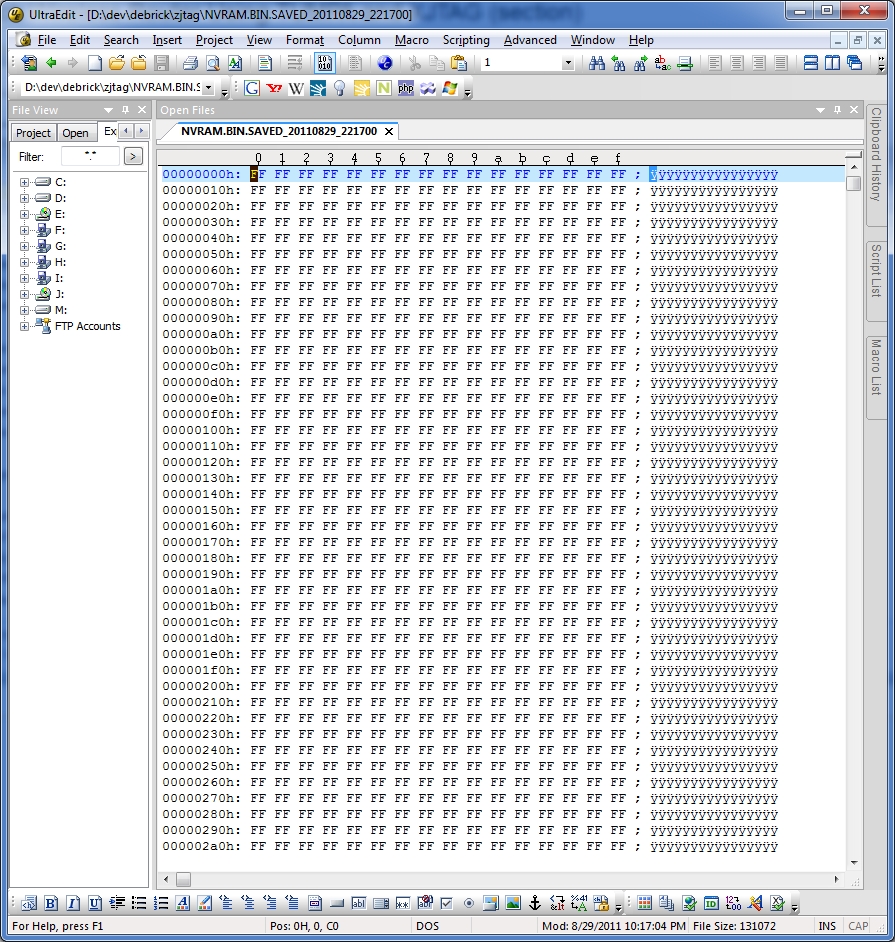
Open the file NVRAM.BIN.SAVED_20110829_221700in any Hex editor (I use UltraEdit), as you see, it is all 0xFF: This should resolve your problem. If this doesn't work, erase the kernel (firmware):
zJTAG -erase:kernel /L1:3then reflash the kernel via TFTP (see TFTP Flashing)
Or still doesn't work, you may need to flash CFE:
zJTAG -flash:CFE /L1:3
The CFE bin files in the repository all have MAC addresses that DO NOT MATCH your hardware, you will need to edit it before you flash it to your router. Please read Debrick Routers Using JTAG Cable first.
Again, to make sure flash is really successful, run a backup command after flash and compare the content with the original one to make sure.
If flash doesn't work or erase doesn't work, try to lower the speed by giving a larger divider, e.g. in my case, use
/L1:4
will decrease TCK to 6Mhz.
One more suggestion is, always backup each area and whole flash before you do anything to it. You never know!
Buy various JTAG cables for your Satellite Receiver, Cable Modem, Wireless Router, Standard Wiggler from http://www.easymg.com and http://www.diygadget.com

10 PCS, 10cm x 10cm, 2 layers prototype for $38.80 shipped!


