TIAO USB Multi Protocol Adapter Lite User's Manual

10 PCS, 10cm x 10cm, 2 layers prototype for $38.80 shipped!
Contents
- 1 Overview
- 2 Technical Specifications
- 3 Board Dimensions
- 4 Board Layout
- 5 Connector Pinout & LEDs
- 5.1 Onboard LEDs
- 5.2 Target Board Power LED
- 5.3 DB9 Male RS232
- 5.4 SPI Connector 1
- 5.5 RS232 Level 2.54mm IDC Header
- 5.6 20 PIN JTAG Connector
- 5.7 MAX3243 Auto Power Down Jumper
- 5.8 Buffer Enable Jumper
- 5.9 Buffer Chip Power Selection Jumper
- 5.10 Serial RS232/TTL level Selection Jumper
- 5.11 TTL Level Serial Connector
- 5.12 SPI Connector 2
- 5.13 PWR/RX/TX LEDs
- 5.14 Target Board Power LED
- 6 Pin Connections
Buy various JTAG cables for your Satellite Receiver, Cable Modem, Wireless Router, Standard Wiggler from http://www.easymg.com and http://www.diygadget.com
Overview
The TIAO USB Multi Protocol Adapter Lite (TUMPA Lite) is a multi-functional USB communication adapter for hobbyists or engineers. The adapter is based on FDTI's flagship communication chip FT232H, a USB 2.0 Hi-Speed (480Mb/s) to UART/FIFO IC. It has one multi-protocol synchronous serial engines (MPSSEs) which allow for communication using JTAG, I2C and SPI on two channels simultaneously.
Technical Specifications
- Single channel USB to serial / parallel ports with a variety of configurations.
- Entire USB protocol handled on the chip. No USB specific firmware programming required.
- USB 2.0 Hi-Speed (480Mbits/Second) and Full Speed (12Mbits/Second) compatible.
- Multi-Protocol Synchronous Serial Engine (MPSSE) to simplify synchronous serial protocol (USB to JTAG, I2C, SPI or bit-bang) design.
- UART transfer data rate up to 12Mbaud. (RS232 Data Rate limited by external level shifter).
- USB to asynchronous 245 FIFO mode for transfer data rate up to 8 MByte/Sec.
- USB to synchronous 245 parallel FIFO mode for transfers up to 40 Mbytes/Sec
- Supports a half duplex FT1248 interface with a configurable width, bi-directional data bus (1, 2, 4 or 8 bits wide).
- CPU-style FIFO interface mode simplifies CPU interface design.
- Fast serial interface option.
- FTDI's royalty-free Virtual Com Port (VCP) and Direct (D2XX) drivers eliminate the requirement for USB driver development in most cases.
- Adjustable receive buffer timeout.
- Option for transmit and receive LED drive signals.
- Bit-bang Mode interface option with RD# and WR strobes
- Highly integrated design includes 5V to 3.3/+1.8V LDO regulator for VCORE, integrated POR function
- Asynchronous serial UART interface option with full hardware handshaking and modem interface signals.
- Fully assisted hardware or X-On / X-Off software handshaking.
- UART Interface supports 7/8 bit data, 1/2 stop bits, and Odd/Even/Mark/Space/No Parity.
- Auto-transmit enable control for RS485 serial applications using TXDEN pin.
- Operation configuration mode and USB Description strings configurable in external EEPROM over the USB interface.
- Configurable I/O drives strength (4, 8, 12 or 16mA) and slew rate.
- Low operating and USB suspend current.
- Supports self powered, bus powered and high-power bus powered USB configurations.
- UHCI/OHCI/EHCI host controller compatible.#
- USB Bulk data transfer mode (512 byte packets in Hi-Speed mode).
- +1.8V (chip core) and +3.3V I/O interfacing (+5V Tolerant).
- Extended -40°C to 85°C industrial operating temperature range.
- Compact 48-pin Lead Free LQFP or QFN package
- Configurable ACBUS I/O pins.
- 4 on-board LEDs / PWR, +3.3V Out, TX and RX
- 1 2x10 20 PIN JTAG header
- 1 2x3 6 PIN SPI 2.54mm IDC header
- 1 SPI MISO pullup config IDC header
- 1 Configurable TX/RX LED IDC header
- On board 3.3V LDO
- USB over-current protection via on-board resetable fuse.
- Strong ESD protection on USB signals.
- Based on the FTDI FT232H USB device.
- Designed for FTDI MPSSE easy-to-use.
- Free drivers for Linux.
- Free drivers for Windows XP, Windows Vista and Windows 7
- Support both 32 bit and 64 bit operating systems
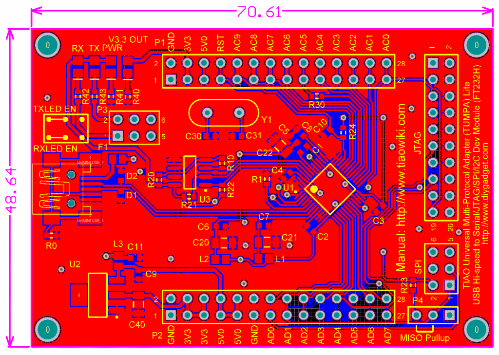
- Board dimension: 48.64mm X 70.61mm (1.91" X 2.78")
Board Dimensions
Board Layout
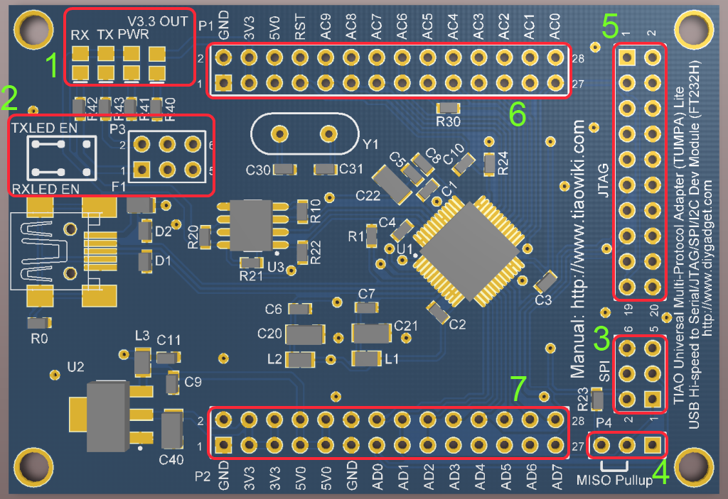
- LEDs - RX/TX/PWR/+3.3V Output
- 2x3 standard 6 PIN 2.54mm IDC for RX/TX LED
- 2x3 PIN 2.54mm IDC SPI header
- SPI pullup enable header
- 2x10 standard 20 PIN 2.54mm IDC JTAG connector
- 2x14 PIN 2.54mm IDC GPIO Pins
- 2x14 PIN 2.54mm IDC GPIO Pins
Connector Pinout & LEDs
Onboard LEDs
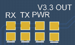
- RX: Indicates FT232H is receiving bytes from target via serial communication channel. See header 2 on how to enable this.
- TX: Indicates FT232H is transmitting bytes to target via serial communication channel. See header 2 on how to enable this.
- PWR: Indicates the TUMPA Lite board is connected to USB port of the computer and FT232H's onboard voltage regulator outputs +3.3V.
- V3.3 Out: Indicates the TUMPA Lite's onboard voltage LDO outputs +3.3V.
Target Board Power LED
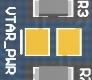
- LED is ON: Target board (PIN 1 of JTAG Header) has power supply > 3.3V.
- LED is OFF: Target board (PIN 1 of JTAG Header) has power supply < 3.3V or no power.
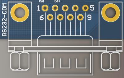
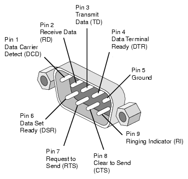
DB9 Male RS232
This connector is enabled only if RS232/TTL jumpers are on RS232-OUT, see Serial RS232/TTL level Selection Jumper
| Pin # | Acronym | Full name | Direction | Description |
|---|---|---|---|---|
| 1 | DCD | Data Carrier Detect | <<-- | Modem connected to another |
| 2 | RxD | Receive Data | <<-- | Receives bytes into PC |
| 3 | TxD | Transmit Data | -->> | Transmits bytes out of PC |
| 4 | DTR | Data Terminal Ready | -->> | I'm ready to communicate |
| 5 | SG | Signal Ground | Ground/GND | |
| 6 | DSR | Data Set Ready | <<-- | I'm ready to communicate |
| 7 | RTS | Request To Send | -->> | RTS/CTS flow control |
| 8 | CTS | Clear To Send | <<-- | RTS/CTS flow control |
| 9 | RI | Ring Indicator | <<-- | Telephone Line Ringing |
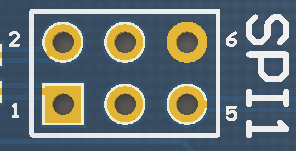
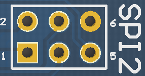
SPI Connector 1
| Pin # | Description |
|---|---|
| 1 | MISO |
| 2 | Vcc (connected to on board 3.3V) |
| 3 | SCK |
| 4 | MOSI |
| 5 | CS |
| 6 | GND |
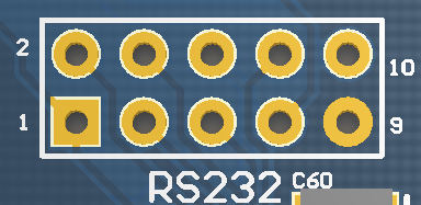
RS232 Level 2.54mm IDC Header
This connector is enabled only if RS232/TTL jumpers are on RS232-OUT, see Serial RS232/TTL level Selection Jumper
For your convenience, we added this header. This header is inter connected to the DB9 connector. The pinout is different then the pinout of DB 9 connector, however the extra pin (PIN 10) is connected to on board 3.3V power. GND pin (PIN 9) and +3.3V PIN (PIN 10) are always enabled regardless the jumpers position of Serial RS232/TTL level Selection Jumper.
This is the pinout of the RS232 level 2.54mm IDC header:
| Pin # | Description |
|---|---|
| 1 | RI |
| 2 | DCD |
| 3 | DSR |
| 4 | CTS |
| 5 | RX |
| 6 | TX |
| 7 | RTS |
| 8 | DTR |
| 9 | GND |
| 10 | +3.3V |
20 PIN JTAG Connector
| Pin # | Description |
|---|---|
| 1 | VTAR |
| 3 | nTRST |
| 5 | TDI |
| 7 | TMS |
| 9 | TCK |
| 11 | RTCK |
| 13 | TDO |
| 15 | RST |
| 17 | DBGRQ |
| 19 | DBGACK |
| 2 | Not Connected |
| 4, 6, 8, 10, 12, 14, 16, 18, 20 | GND |
MAX3243 Auto Power Down Jumper
This jumper controls whether to always enable MAX3243 or let FT2232H automatically enables it (save power).
- Jumper on PIN 1 and PIN 2: Always enable MAX3243
- Jumper on PIN 2 and PIN 3: FT2232H (PWREN, PIN 60)controls when to enable or disable MAX3243.
Buffer Enable Jumper
This jumper controls whether to software enable/disable buffer chip (74LVC16T254).
- Jumper on PIN 1 and PIN 2: Enable (Low)/Disable (High) 74LVC16T245 via FT2232H's ACBUS3 (PIN 29).
- Jumper on PIN 2 and PIN 3: Always enable 74LVC16T245
Buffer Chip Power Selection Jumper
This jumper controls how to power the buffer / voltage translator chip (74LVC16T245)
The 74LVC16T245's Vcc(A) is connected to on board +3.3V. You can either power the Vcc(B) using on board +3.3V or powered by the target board. If powered by target board, please make sure the target board's power is in the range of +1.8V - +5.5V.
- Jumper on PIN 1 and PIN 2: Power the buffer chip 74LVC16T245's Vcc(B) via the on board +3.3V source.
- Jumper on PIN 2 and PIN 3: Power the buffer chio 74LVC16T245's Vcc(B) by target board. (PIN 3 of this header is connected to JTAG header's PIN 1)
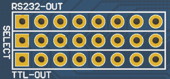
Serial RS232/TTL level Selection Jumper
These jumpers allows you to have serial communication at either RS232 level or TTL level.
- Jumpers short top row (RS232-OUT) and middle row (SELECT) (this is the default): enable RS232 level serial output. (thus DB9 Connector and RS232 Level 2.54mm IDC Header are enabled)
- Jumpers short middle row (SELECT)and bottom row (TTL-OUT): enable TTL level serial output. (thus TTL Level Serial Connectoris enabled)
TTL Level Serial Connector
This connector is enabled only if RS232/TTL jumpers are on TTL-OUT, see Serial RS232/TTL level Selection Jumper
| Pin # | Description |
|---|---|
| 1 | Tx |
| 2 | Rx |
| 3 | RTS |
| 4 | CTS |
| 5 | DTR |
| 6 | DSR |
| 7 | DCD |
| 8 | RI |
| 9 | +3.3V |
| 10 | +5V (USB Power) |
| 11, 12 | GND |
The power pins (9, 10, 11 and 12) are always connected, regardless of the jumper positions of Serial RS232/TTL level Selection Jumper.
SPI Connector 2
| Pin # | Description |
|---|---|
| 1 | MISO |
| 2 | Vcc (connected to on board 3.3V) |
| 3 | SCK |
| 4 | MOSI |
| 5 | CS |
| 6 | GND |
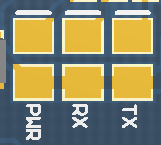
PWR/RX/TX LEDs
- PWR: indicates the TUMPA board is connected to USB port of the computer and on board voltage regulator outputs +3.3V.
- RX: Indicates FT2232H is receiving bytes from target via serial communication channel B
- TX: Indicates FT2232H is transmitting bytes to target via serial communication channel B
Target Board Power LED
- LED is ON: Target board (PIN 1 of JTAG Header) has power supply > 3.3V.
- LED is OFF: Target board (PIN 1 of JTAG Header) has power supply < 3.3V or no power.
The VTAR can also be detected by software. If VTAR has voltage > 3.3V, ACBUS4 (PIN 30) of FT2232H will be LOW. Otherwise it will be HIGH.
Pin Connections
| FT2232H | 20 PIN JTAG Header | SPI Header 1 | DB9 Connector | RS232 Level Output Header | TTL Level Output Header | SPI Header 2 | Memo |
| ADBUS0 | TCK | SCK | |||||
| ADBUS1 | TDI | MOSI | |||||
| ADBUS2 | TDO | MISO | |||||
| ADBUS3 | TMS | CS | |||||
| ADBUS4 | RST | ||||||
| ADBUS5 | nTRST | ||||||
| ADBUS6 | DBGRQ | ||||||
| ADBUS7 | RTCK | ||||||
| ACBUS0 | DBGACK | ||||||
| ACBUS1 | Connected to nTRST pin of JTAG Header, (input) | ||||||
| ACBUS2 | Connected to RST pin of JTAG Header, as (input) | ||||||
| ACBUS3 | OEN Pin (enable buffer chip), active low (output) | ||||||
| ACBUS4 | Target present pin. Detect VTAR, active low (input) | ||||||
| ACBUS5 | |||||||
| ACBUS6 | |||||||
| ACBUS7 | |||||||
| BDBUS0 | TX | TX | TX | SCK | |||
| BDBUS1 | RX | RX | RX | MOSI | |||
| BDBUS2 | RTS | RTS | RTS | MISO | |||
| BDBUS3 | CTS | CTS | CTS | CS | |||
| BDBUS4 | DTR | DTR | DTR | ||||
| BDBUS5 | DSR | DSR | DSR | ||||
| BDBUS6 | DCD | DCD | DCD | ||||
| BDBUS7 | RI | RI | RI | ||||
| BCBUS0 | |||||||
| BCBUS1 | |||||||
| BCBUS2 | |||||||
| BCBUS3 | RX LED | ||||||
| BCBUS4 | TX LED | ||||||
| BCBUS5 | |||||||
| BCBUS6 | |||||||
| BCBUS7 | |||||||
| PWREN | Enable MAX3243. Active low (output) |
Buy various JTAG cables for your Satellite Receiver, Cable Modem, Wireless Router, Standard Wiggler from http://www.easymg.com and http://www.diygadget.com

10 PCS, 10cm x 10cm, 2 layers prototype for $38.80 shipped!
