Difference between revisions of "TIAO GBoard/GIMX Board Hardware Layout"
From TIAO's Wiki

10 PCS, 10cm x 10cm, 2 layers prototype for $38.80 shipped!
(→TIAO GBoard/GIMX Adapter Connector Layouts) |
(→J5) |
||
| (7 intermediate revisions by the same user not shown) | |||
| Line 5: | Line 5: | ||
For system connection diagram as GIMX adapter, please refer to [[TIAO GIMX System Connection Diagram]]. | For system connection diagram as GIMX adapter, please refer to [[TIAO GIMX System Connection Diagram]]. | ||
| + | For loading the firmware, please refer to [[How to Install GIMX Firmware on TIAO GBoard/GIMX Adapter]] | ||
The [http://www.diygadget.com/development-boards/tiao-gimx-gboard-game-input-multiplexer-matrix-usb-serial-and-atmega32u4-development-board.html TIAO GBoard / GIMX adapter] is a combined all in one board for serial and AVR development. It also provides jumper connections for easy and quick GIMX connectoion (to be used as a GIMX Game Input MultipleXer or Game Input MatriX adapter. For more information on GIMX, please check it out [http://blog.gimx.fr/ here]. | The [http://www.diygadget.com/development-boards/tiao-gimx-gboard-game-input-multiplexer-matrix-usb-serial-and-atmega32u4-development-board.html TIAO GBoard / GIMX adapter] is a combined all in one board for serial and AVR development. It also provides jumper connections for easy and quick GIMX connectoion (to be used as a GIMX Game Input MultipleXer or Game Input MatriX adapter. For more information on GIMX, please check it out [http://blog.gimx.fr/ here]. | ||
| Line 30: | Line 31: | ||
# [[#J1|USB to COM RX LED]] | # [[#J1|USB to COM RX LED]] | ||
| − | # [[#J2|USB to COM | + | # [[#J2|USB to COM TX LED]] |
# [[#J3|GIMX TXD Enable]] | # [[#J3|GIMX TXD Enable]] | ||
# [[#J4|GIMX RXD Enable]] | # [[#J4|GIMX RXD Enable]] | ||
| Line 39: | Line 40: | ||
# [[#ATMEGA32U4 IO Pin Header 2|ATMEGA32U4 IO Pin Header 2]] | # [[#ATMEGA32U4 IO Pin Header 2|ATMEGA32U4 IO Pin Header 2]] | ||
# [[#FT231X IO Pin Header|FT231X IO Pin Header]] | # [[#FT231X IO Pin Header|FT231X IO Pin Header]] | ||
| + | # [[#ATMEGA32U4 Bootloader Pin|ATMEGA32U4 Bootloader Pin]] | ||
| + | ==== J1 ==== | ||
| + | [[Image:gimx-j1.png||none]] | ||
| − | ==== | + | * Jumper on: Enable RX Led for USB to COM/Serial. |
| − | [[Image: | + | * Jumper off: Enable CBUS1 output for FT231X. |
| + | |||
| + | |||
| + | ==== J2 ==== | ||
| + | [[Image:gimx-j2.png||none]] | ||
| + | |||
| + | * Jumper on: Enable TX Led for USB to COM/Serial. | ||
| + | * Jumper off: Enable CBUS2 output for FT231X. | ||
| + | |||
| + | ==== J3 ==== | ||
| + | [[Image:gimx-j3.png||none]] | ||
| + | |||
| + | * Jumper on: Enable board to be a DIY GIMX adapter (J4 has to be on as well) | ||
| + | * Jumper off: Enable board to be a AVR and USB to Serial development board. (J4 has to be off as well) | ||
| + | |||
| + | ==== J4 ==== | ||
| + | [[Image:gimx-j4.png||none]] | ||
| + | |||
| + | * Jumper on: Enable board to be a DIY GIMX adapter (J3 has to be on as well) | ||
| + | * Jumper off: Enable board to be a AVR and USB to Serial development board. (J3 has to be off as well) | ||
| + | |||
| + | |||
| + | ==== J5 ==== | ||
| + | [[Image:gimx-j5.png||none]] | ||
| + | |||
| + | * Jumper on 1-2: Enable 5.0V IO on ATMEGA32U4. | ||
| + | * Jumper on 2-3: Enable 3.3V IO on ATMEGA32U4. | ||
| + | |||
| + | ==== ATMEGA32U4 USB Connector ==== | ||
| + | [[Image:gimx-6.png||none]] | ||
| + | |||
| + | * The USB connector for ATMEGA32U4. | ||
| + | ==== FT232X USB Connector ==== | ||
| + | [[Image:gimx-7.png||none]] | ||
| + | |||
| + | * The USB connector for FT231X. | ||
| + | |||
| + | ==== ATMEGA32U4 IO Pin Header 1 ==== | ||
| + | |||
| + | [[Image:gimx-8.png|none]] | ||
{| | {| | ||
! align="left"|Pin # | ! align="left"|Pin # | ||
| − | ! | + | ! ATMEGA32U4 Pin |
|- | |- | ||
| 1 | | 1 | ||
| − | | | + | | GND |
|- | |- | ||
| 2 | | 2 | ||
| − | | | + | | +5V |
|- | |- | ||
| 3 | | 3 | ||
| − | | | + | | RST (Low) |
|- | |- | ||
| 4 | | 4 | ||
| − | | | + | | PE6 |
|- | |- | ||
| 5 | | 5 | ||
| − | | | + | | PB0 |
|- | |- | ||
| 6 | | 6 | ||
| − | | | + | | PB1 |
|- | |- | ||
| 7 | | 7 | ||
| − | | | + | | PB2 |
|- | |- | ||
| 8 | | 8 | ||
| − | | | + | | PB3 |
|- | |- | ||
| 9 | | 9 | ||
| − | | | + | | PB7 |
|- | |- | ||
| 10 | | 10 | ||
| − | | | + | | PD0 |
|- | |- | ||
| 11 | | 11 | ||
| − | | | + | | PD1 |
|- | |- | ||
| 12 | | 12 | ||
| Line 83: | Line 126: | ||
|- | |- | ||
| 13 | | 13 | ||
| − | | | + | | PD5 |
|- | |- | ||
| 14 | | 14 | ||
| − | | | + | | PD3 |
|- | |- | ||
| 15 | | 15 | ||
| − | | | + | | PC6 |
|- | |- | ||
| 16 | | 16 | ||
| − | | | + | | PC7 |
| − | |||
| − | |||
| − | |||
| − | |||
| − | |||
| − | |||
|} | |} | ||
| − | ==== | + | ==== ATMEGA32U4 IO Pin Header 2 ==== |
| − | |||
| − | |||
| − | + | [[Image:gimx-9.png|none]] | |
| − | [[Image: | ||
{| | {| | ||
! align="left"|Pin # | ! align="left"|Pin # | ||
| − | ! | + | ! ATMEGA32U4 Pin |
|- | |- | ||
| 1 | | 1 | ||
| − | |||
| − | |||
| − | |||
| − | |||
| − | |||
| − | |||
| GND | | GND | ||
| − | |||
| − | |||
| − | |||
| − | |||
| − | |||
| − | |||
| − | |||
| − | |||
| − | |||
| − | |||
| − | |||
| − | |||
| − | |||
|- | |- | ||
| 2 | | 2 | ||
| − | | | + | | Vcc (5.0 or 3.3 depending on J5) |
|- | |- | ||
| 3 | | 3 | ||
| − | | | + | | Vcc (5.0 or 3.3 depending on J5) |
|- | |- | ||
| 4 | | 4 | ||
| − | | | + | | AREF |
|- | |- | ||
| 5 | | 5 | ||
| − | | | + | | PF0 |
|- | |- | ||
| 6 | | 6 | ||
| − | | | + | | PF1 |
| + | |- | ||
| + | | 7 | ||
| + | | PF4 | ||
| + | |- | ||
| + | | 8 | ||
| + | | PF5 | ||
| + | |- | ||
| + | | 9 | ||
| + | | PF6 | ||
| + | |- | ||
| + | | 10 | ||
| + | | PF7 | ||
| + | |- | ||
| + | | 11 | ||
| + | | PB6 | ||
| + | |- | ||
| + | | 12 | ||
| + | | PB5 | ||
| + | |- | ||
| + | | 13 | ||
| + | | PB4 | ||
| + | |- | ||
| + | | 14 | ||
| + | | PD7 | ||
| + | |- | ||
| + | | 15 | ||
| + | | PD6 | ||
| + | |- | ||
| + | | 16 | ||
| + | | PD4 | ||
|} | |} | ||
| − | |||
| − | |||
| + | ==== FT231X IO Pin Header ==== | ||
| + | |||
| + | [[Image:Gimx-10.png||None]] | ||
{| | {| | ||
! align="left"|Pin # | ! align="left"|Pin # | ||
| − | ! | + | ! FT231X Pin |
|- | |- | ||
| 1 | | 1 | ||
| − | | | + | | RTS |
|- | |- | ||
| 2 | | 2 | ||
| − | | | + | | DTR |
|- | |- | ||
| 3 | | 3 | ||
| − | | | + | | RI |
|- | |- | ||
| 4 | | 4 | ||
| − | | | + | | RXD |
|- | |- | ||
| 5 | | 5 | ||
| − | | | + | | DSR |
|- | |- | ||
| 6 | | 6 | ||
| − | | | + | | DCD |
|- | |- | ||
| 7 | | 7 | ||
| − | | | + | | TXLED/CBUS2 |
|- | |- | ||
| 8 | | 8 | ||
| − | | | + | | CTS |
| − | |||
| − | |||
| − | |||
| − | |||
| − | |||
| − | |||
| − | |||
| − | |||
| − | |||
| − | |||
| − | |||
| − | |||
| − | |||
| − | |||
| − | |||
| − | |||
| − | |||
| − | |||
| − | |||
| − | |||
| − | |||
|- | |- | ||
| − | | | + | | 9 |
| − | | | + | | RXLED/CBUS1 |
|- | |- | ||
| − | | | + | | 10 |
| − | | | + | | CBUS0 |
|- | |- | ||
| − | | | + | | 11 |
| − | | | + | | CBUS3 |
| − | |||
| − | |||
| − | |||
| − | |||
| − | |||
| − | |||
| − | |||
| − | |||
| − | |||
| − | |||
| − | |||
| − | |||
|- | |- | ||
| − | | | + | | 12 |
| − | | | + | | TXD |
| − | |||
| − | |||
| − | |||
| − | |||
| − | |||
| − | |||
| − | |||
| − | |||
| − | |||
|- | |- | ||
| − | | | + | | 13 |
| − | | | + | | V5 |
| − | |||
| − | |||
| − | |||
| − | |||
| − | |||
| − | |||
| − | |||
| − | |||
| − | |||
| − | |||
| − | |||
| − | |||
| − | |||
| − | |||
| − | |||
| − | |||
| − | |||
| − | |||
| − | |||
| − | |||
| − | |||
| − | |||
| − | |||
| − | |||
| − | |||
| − | |||
| − | |||
| − | |||
| − | |||
| − | |||
| − | |||
| − | |||
| − | |||
| − | |||
| − | |||
| − | |||
| − | |||
| − | |||
| − | |||
| − | |||
| − | |||
| − | |||
| − | |||
| − | |||
| − | |||
| − | |||
| − | |||
| − | |||
|- | |- | ||
| + | | 14 | ||
| V33 | | V33 | ||
| − | |||
| − | |||
| − | |||
| − | |||
| − | |||
| − | |||
| − | |||
| − | |||
| − | |||
| − | |||
| − | |||
| − | |||
| − | |||
| − | |||
|- | |- | ||
| − | | | + | | 15 |
| − | | | + | | GND |
|- | |- | ||
| − | | | + | | 16 |
| − | |||
| − | |||
| − | |||
| GND | | GND | ||
| − | |||
| − | |||
| − | |||
|} | |} | ||
| − | ==== | + | ==== ATMEGA32U4 Bootloader Pin ==== |
| − | |||
| − | |||
| − | |||
| − | * | + | * ATMEGA32U4 Bootloader Pin, press and hold to enter bootloader mode. |
| − | |||
| − | |||
| − | |||
Latest revision as of 11:16, 9 June 2016
Contents
TIAO GBoard / GIMX Adapter
For system connection diagram as GIMX adapter, please refer to TIAO GIMX System Connection Diagram. For loading the firmware, please refer to How to Install GIMX Firmware on TIAO GBoard/GIMX Adapter
The TIAO GBoard / GIMX adapter is a combined all in one board for serial and AVR development. It also provides jumper connections for easy and quick GIMX connectoion (to be used as a GIMX Game Input MultipleXer or Game Input MatriX adapter. For more information on GIMX, please check it out here.
The TIAO GBoard/GIMX Adapter features:
- All in one board contains USB to COM adapter and ATMEVA32U4 for AVR development.
- Bootloader is installed on the ATMEGA32U4, so you don't need a programmer to load the firmware.
- Quick connection jumpers to convert the GBoard to a GIMX adapter
- RX/TX LED, enable LEDs or use the pins for IO ports
TIAO GBoard/GIMX Adapter Hardware Dimensions
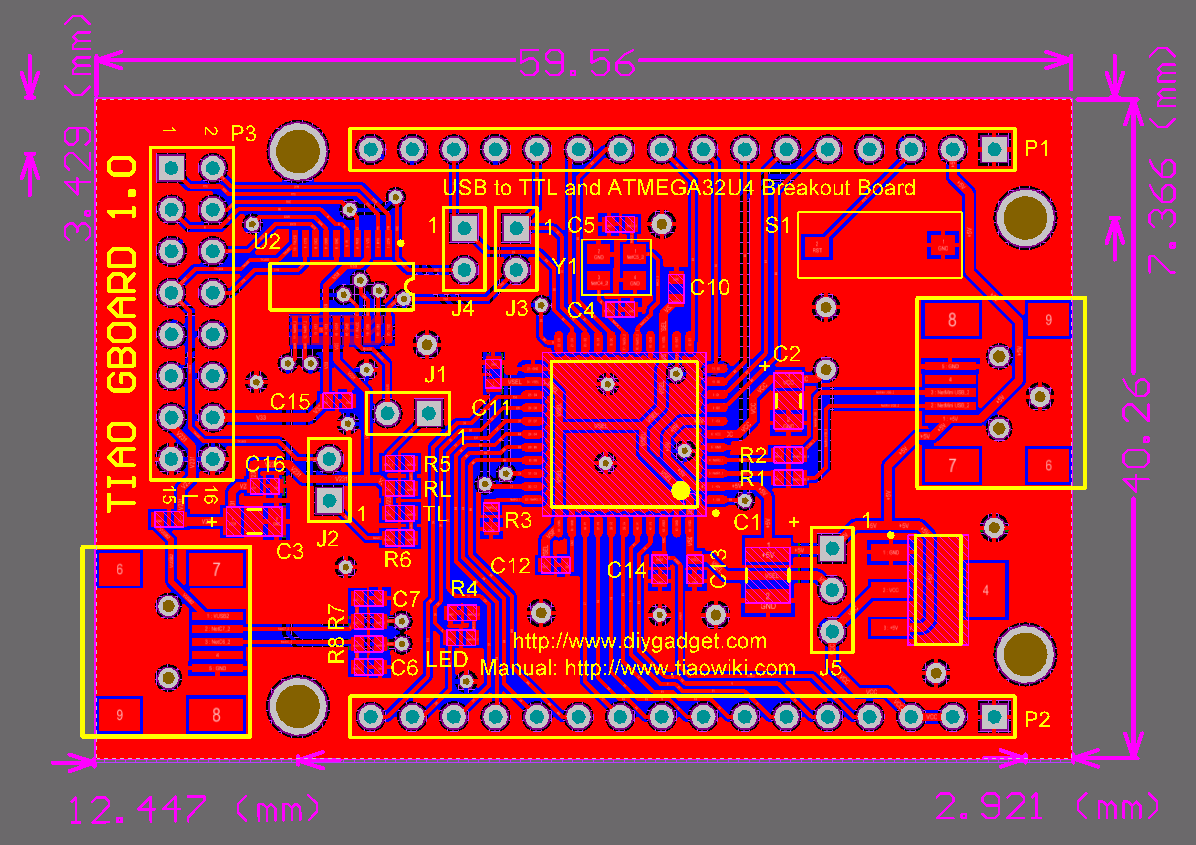
The board dimension of TSS is 59.56 x 40.26mm. It also has 4 mounting holes, the radius of the mounting hole is 2.5mm:
TIAO GBoard/GIMX Adapter Connector Layouts
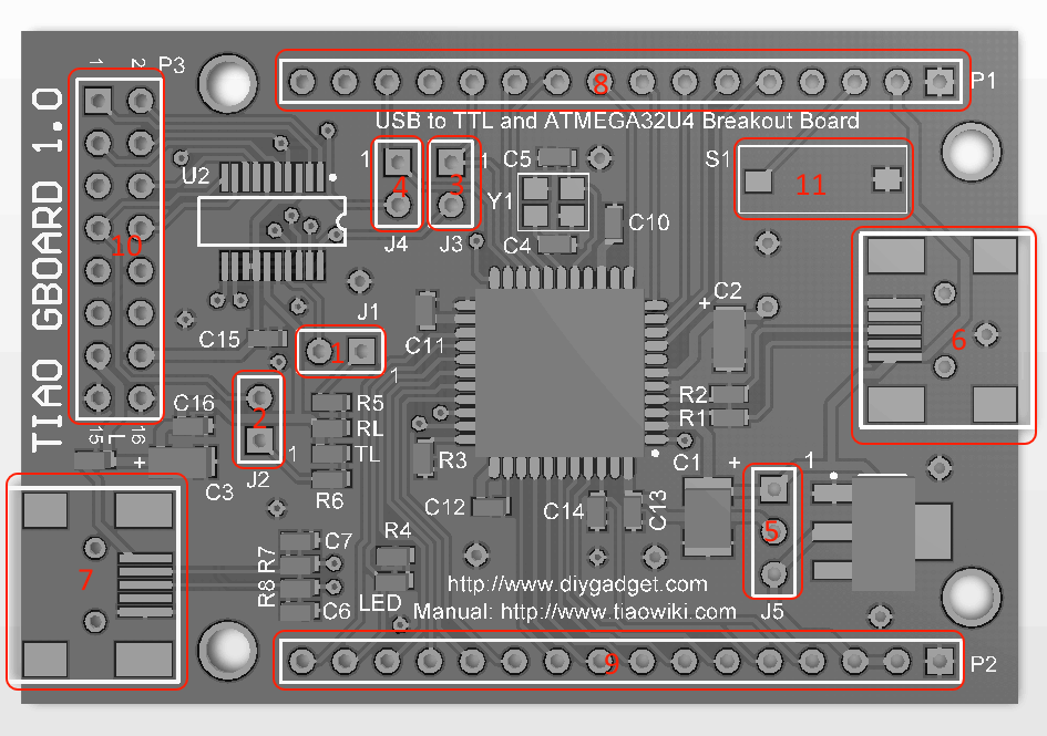
The following picture shows the connector layout of the TIAO GBoard/GIMX Adapter.
- USB to COM RX LED
- USB to COM TX LED
- GIMX TXD Enable
- GIMX RXD Enable
- ATMEGA32U4 Power Select
- ATMEGA32U4 USB Connector
- FT231X USB Connector
- ATMEGA32U4 IO Pin Header 1
- ATMEGA32U4 IO Pin Header 2
- FT231X IO Pin Header
- ATMEGA32U4 Bootloader Pin
J1
- Jumper on: Enable RX Led for USB to COM/Serial.
- Jumper off: Enable CBUS1 output for FT231X.
J2
- Jumper on: Enable TX Led for USB to COM/Serial.
- Jumper off: Enable CBUS2 output for FT231X.
J3
- Jumper on: Enable board to be a DIY GIMX adapter (J4 has to be on as well)
- Jumper off: Enable board to be a AVR and USB to Serial development board. (J4 has to be off as well)
J4
- Jumper on: Enable board to be a DIY GIMX adapter (J3 has to be on as well)
- Jumper off: Enable board to be a AVR and USB to Serial development board. (J3 has to be off as well)
J5
- Jumper on 1-2: Enable 5.0V IO on ATMEGA32U4.
- Jumper on 2-3: Enable 3.3V IO on ATMEGA32U4.
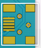
ATMEGA32U4 USB Connector
- The USB connector for ATMEGA32U4.
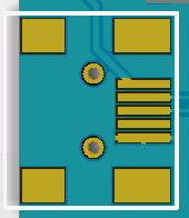
FT232X USB Connector
- The USB connector for FT231X.
ATMEGA32U4 IO Pin Header 1
| Pin # | ATMEGA32U4 Pin |
|---|---|
| 1 | GND |
| 2 | +5V |
| 3 | RST (Low) |
| 4 | PE6 |
| 5 | PB0 |
| 6 | PB1 |
| 7 | PB2 |
| 8 | PB3 |
| 9 | PB7 |
| 10 | PD0 |
| 11 | PD1 |
| 12 | PD2 |
| 13 | PD5 |
| 14 | PD3 |
| 15 | PC6 |
| 16 | PC7 |
ATMEGA32U4 IO Pin Header 2
| Pin # | ATMEGA32U4 Pin |
|---|---|
| 1 | GND |
| 2 | Vcc (5.0 or 3.3 depending on J5) |
| 3 | Vcc (5.0 or 3.3 depending on J5) |
| 4 | AREF |
| 5 | PF0 |
| 6 | PF1 |
| 7 | PF4 |
| 8 | PF5 |
| 9 | PF6 |
| 10 | PF7 |
| 11 | PB6 |
| 12 | PB5 |
| 13 | PB4 |
| 14 | PD7 |
| 15 | PD6 |
| 16 | PD4 |
FT231X IO Pin Header
| Pin # | FT231X Pin |
|---|---|
| 1 | RTS |
| 2 | DTR |
| 3 | RI |
| 4 | RXD |
| 5 | DSR |
| 6 | DCD |
| 7 | TXLED/CBUS2 |
| 8 | CTS |
| 9 | RXLED/CBUS1 |
| 10 | CBUS0 |
| 11 | CBUS3 |
| 12 | TXD |
| 13 | V5 |
| 14 | V33 |
| 15 | GND |
| 16 | GND |
ATMEGA32U4 Bootloader Pin
- ATMEGA32U4 Bootloader Pin, press and hold to enter bootloader mode.

10 PCS, 10cm x 10cm, 2 layers prototype for $38.80 shipped!


