Difference between revisions of "TIAO USB Multi Protocol Adapter User's Manual"

10 PCS, 10cm x 10cm, 2 layers prototype for $38.80 shipped!
(→20 PIN JTAG Connector) |
|||
| (88 intermediate revisions by the same user not shown) | |||
| Line 1: | Line 1: | ||
| + | <meta name="keywords" content="TIAOWIKI,JTAG,TJTAG,FTA,JTAG,WRT54G,DD-WRT,urjtag, openocd, flashrom,USB jtag, debrick,tomato,router,wireless router,motorola modem,sb5100,wiggler,arm,mips,avr,buffered jtag,unbuffered jtag,10 pin,20 pin, 12 pin,xbox,xbox 360,modchip mod-chip,mod chip,liteon,lite-on,samsung,hitachi,lg,dvd rom,sata,dvd key,usb probe,cable modem, usb spear,serial spear, serial probe, extract dvd key,mod xbox 360,video games"></meta> | ||
| + | <meta name="description" content="TIAOWIKI tutorials on how to fix your fta receiver, debrick your wireless router, fix you cable modem, mod your xbox 360, extract the xbox 360 dvd key, flash xbox 360 dvd firmware, flash ixtreme firmware"></meta> | ||
| + | |||
| + | __TOC__ | ||
| + | |||
| + | <span class="plainlinks"> | ||
| + | |||
| + | <include nopre noesc src="/home/tiao/public_html/tiaowiki/wiki/extensions/include/jtag.inc"/> | ||
| + | |||
| + | Buy various JTAG cables for your Satellite Receiver, Cable Modem, Wireless Router, Standard Wiggler from [http://www.easymg.com http://www.easymg.com] and [http://www.diygadget.com http://www.diygadget.com] | ||
| + | </span> | ||
| + | |||
| + | |||
| + | |||
= Overview = | = Overview = | ||
| − | The TIAO USB Multi Protocol Adapter (TUMPA) is a multi-functional USB communication adapter for hobbyists or engineers. | + | The [https://www.diygadget.com/jtag-cables-and-microcontroller-programmers/114-tiao-usb-multi-protocol-adapter-jtag-spi-i2c-serial.html TIAO USB Multi Protocol Adapter (TUMPA)] is a multi-functional USB communication adapter for hobbyists or engineers. |
The adapter is based on FDTI's flagship communication chip FT2232H, a USB 2.0 Hi-Speed (480Mb/s) to UART/FIFO IC. It has two multi-protocol synchronous serial engines (MPSSEs) which allow for communication using JTAG, I2C and SPI on two channels simultaneously. | The adapter is based on FDTI's flagship communication chip FT2232H, a USB 2.0 Hi-Speed (480Mb/s) to UART/FIFO IC. It has two multi-protocol synchronous serial engines (MPSSEs) which allow for communication using JTAG, I2C and SPI on two channels simultaneously. | ||
| + | |||
| + | Looking for PDF version of this manual? It is here: | ||
| + | |||
| + | [http://www.tiaowiki.com/download//file.php?id=38 Download PDF version of this manual] | ||
| + | |||
| + | Thanks to stealther for creating the PDF manual. | ||
= Technical Specifications = | = Technical Specifications = | ||
| − | + | * SWD support (Added in V2) | |
| + | * RST line jumper header (added in V2) | ||
* USB 2.0 Hi-Speed (480Mb/s) | * USB 2.0 Hi-Speed (480Mb/s) | ||
* JTAG / IEEE 1149.1 compatible. | * JTAG / IEEE 1149.1 compatible. | ||
| Line 35: | Line 56: | ||
* Support both 32 bit and 64 bit operating systems | * Support both 32 bit and 64 bit operating systems | ||
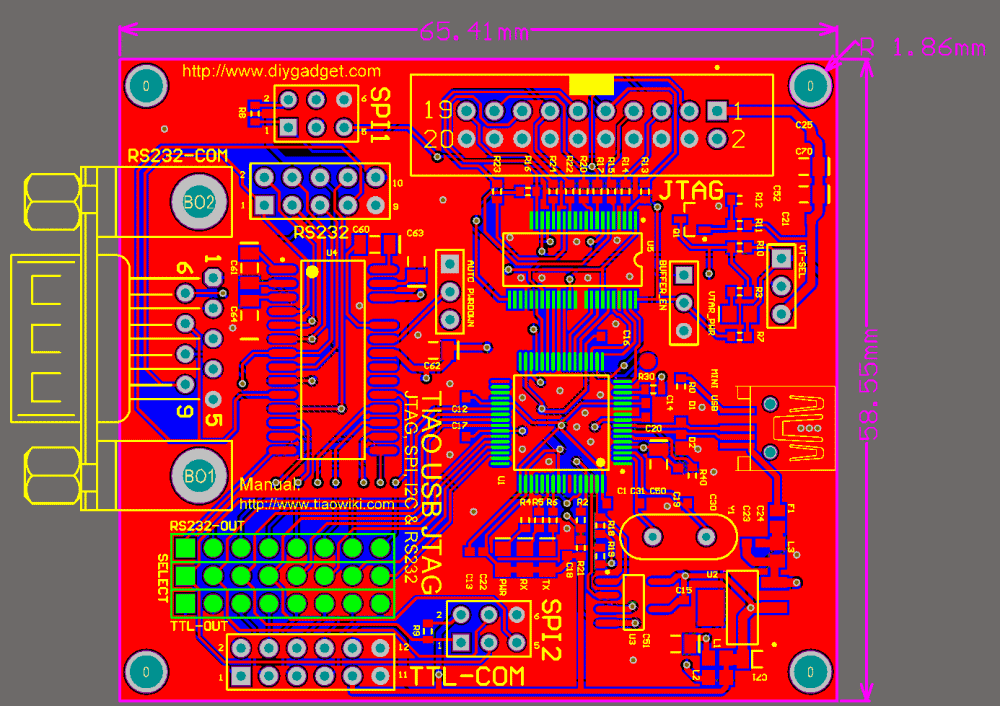
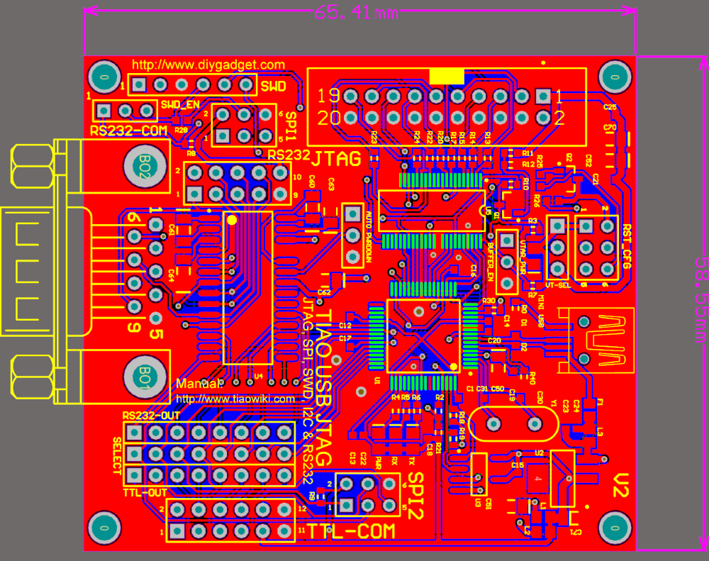
* Board dimension: 65.41mm X 58.55mm (2.58" X 2.31") | * Board dimension: 65.41mm X 58.55mm (2.58" X 2.31") | ||
| + | |||
| + | = Board Dimensions = | ||
| + | |||
| + | V1: | ||
| + | [[Image:Tumpa.dimension.gif|none]] | ||
| + | |||
| + | V2: | ||
| + | [[Image:Tumpav2-d.png|none]] | ||
= Board Layout = | = Board Layout = | ||
| + | V1: | ||
[[Image:tumpa.board.layout.png|none]] | [[Image:tumpa.board.layout.png|none]] | ||
| + | |||
| + | V2: | ||
| + | [[Image:tumpav2-layout.png|none]] | ||
# [[#DB9_Male_RS232|DB9 male RS232 connector (Channel B)]] | # [[#DB9_Male_RS232|DB9 male RS232 connector (Channel B)]] | ||
# [[#SPI_Connector_1|2x3 standard 6 PIN 2.54mm IDC SPI connector (Channel A)]] | # [[#SPI_Connector_1|2x3 standard 6 PIN 2.54mm IDC SPI connector (Channel A)]] | ||
| − | # 2x10 standard 20 PIN 2.54mm IDC JTAG connector (Channel A) | + | # [[#RS232_Level_2.54mm_IDC_Header|RS232 Level 2.54mm IDC Header]] |
| − | # Auto power down jumper header for MAX3243 (force on or auto power down). Default force on (jumper is on pin 1and 2) | + | # [[#20_PIN_JTAG_Connector|2x10 standard 20 PIN 2.54mm IDC JTAG connector (Channel A)]] |
| − | # Buffer enable jumper header for 74LVC16T245. Default is always enabled. (jumper on pin 2 and 3) | + | # [[#MAX3243_Auto_Power_Down_Jumper|Auto power down jumper header for MAX3243 (force on or auto power down). Default force on (jumper is on pin 1and 2)]] |
| − | # | + | # [[#Buffer_Enable_Jumper|Buffer enable jumper header for 74LVC16T245. Default is always enabled. (jumper on pin 2 and 3)]] |
| − | # 3x8 PIN RS232 or TTL level serial communication jumpmer. Default is RS232 output (jumpers short | + | # [[#Buffer_Chip_Power_Selection_Jumper|Buffer chip 74LVC16T245 Vcc(B) power select jumper. Default is to power Vcc(B) by TUMPA (3.3V only) (jumper on pin 1 and 2)]] |
| − | # 2x6 PIN TTL level 2.54mm IDC serial header (channel B) | + | # [[#Serial_RS232/TTL_level_Selection_Jumper|3x8 PIN RS232 or TTL level serial communication jumpmer. Default is RS232 output (jumpers short top row and middle rows) (Channel B)]] |
| − | # 2x3 PIN 2.54mm IDC SPI header (channel B) | + | # [[#TTL_Level_Serial_Connector|2x6 PIN TTL level 2.54mm IDC serial header (channel B)]] |
| − | # | + | # [[#SPI_Connector_2|2x3 PIN 2.54mm IDC SPI header (channel B)]] |
| − | # Status LEDs. From left to right: Power (indicates TUMPA is powered on), RX and TX. | + | # [[#PWR/RX/TX_LEDs|Status LEDs. From left to right: Power (indicates TUMPA is powered on), RX and TX]] |
| + | # [[#Target_Board_Power_LED|Target board power LED. Indicates target board has power]] | ||
| + | # [[#RST_signal_polarity_select|RST signal polarity select. Change the RST signal polarity]] | ||
| + | # [[#SWD_Enable_Jumper|SWD Enable Jumper. Enable or disable SWD]] | ||
| + | # [[#SWD_Header|SWD header. Header for SWD]] | ||
| − | = Connector Pinout = | + | = Connector Pinout & LEDs = |
== DB9 Male RS232 == | == DB9 Male RS232 == | ||
| − | '''This connector is enabled only if RS232/TTL jumpers are on RS232-OUT''' | + | '''This connector is enabled only if RS232/TTL jumpers are on RS232-OUT, see [[#Serial_RS232/TTL_level_Selection_Jumper|Serial RS232/TTL level Selection Jumper]]''' |
[[Image:Tumpa.rs232.connector.1.png|middle]][[Image:Tumpa.rs232.connector.2.png|middle]] | [[Image:Tumpa.rs232.connector.1.png|middle]][[Image:Tumpa.rs232.connector.2.png|middle]] | ||
| Line 149: | Line 186: | ||
|} | |} | ||
| + | == RS232 Level 2.54mm IDC Header == | ||
| + | |||
| + | '''This connector is enabled only if RS232/TTL jumpers are on RS232-OUT, see [[#Serial_RS232/TTL_level_Selection_Jumper|Serial RS232/TTL level Selection Jumper]]''' | ||
| + | |||
| + | [[Image:tumpa.rs232.connector.png|none]] | ||
| + | |||
| + | For your convenience, we added this header. This header is inter connected to the DB9 connector. The pinout is different then the pinout of [[#DB9_Male_RS232|DB 9 connector]], however the extra pin (PIN 10) is connected to on board 3.3V power. GND pin (PIN 9) and +3.3V PIN (PIN 10) are always enabled regardless the jumpers position of [[#Serial_RS232/TTL_level_Selection_Jumper|Serial RS232/TTL level Selection Jumper]]. | ||
| + | |||
| + | This is the pinout of the RS232 level 2.54mm IDC header: | ||
| + | |||
| + | |||
| + | {| | ||
| + | ! align="left"|Pin # | ||
| + | ! Description | ||
| + | |- | ||
| + | | 1 | ||
| + | | RI | ||
| + | |- | ||
| + | | 2 | ||
| + | | DCD | ||
| + | |- | ||
| + | | 3 | ||
| + | | DSR | ||
| + | |- | ||
| + | | 4 | ||
| + | | CTS | ||
| + | |- | ||
| + | | 5 | ||
| + | | RX | ||
| + | |- | ||
| + | | 6 | ||
| + | | TX | ||
| + | |- | ||
| + | | 7 | ||
| + | | RTS | ||
| + | |- | ||
| + | | 8 | ||
| + | | DTR | ||
| + | |- | ||
| + | | 9 | ||
| + | | GND | ||
| + | |- | ||
| + | | 10 | ||
| + | | +3.3V | ||
| + | |} | ||
== 20 PIN JTAG Connector == | == 20 PIN JTAG Connector == | ||
| Line 190: | Line 272: | ||
| 2 | | 2 | ||
| Not Connected | | Not Connected | ||
| + | |- | ||
| 4, 6, 8, 10, 12, 14, 16, 18, 20 | | 4, 6, 8, 10, 12, 14, 16, 18, 20 | ||
| GND | | GND | ||
|} | |} | ||
| + | |||
| + | |||
| + | |||
| + | == MAX3243 Auto Power Down Jumper == | ||
| + | |||
| + | [[Image:Tumpa.auto.power.down.max3243.1.png|none]] | ||
| + | |||
| + | This jumper controls whether to always enable MAX3243 or let FT2232H automatically enables it (save power). | ||
| + | |||
| + | * Jumper on PIN 1 and PIN 2: Always enable MAX3243 | ||
| + | * Jumper on PIN 2 and PIN 3: FT2232H (<span style="text-decoration: overline">PWREN</span>, PIN 60)controls when to enable or disable MAX3243. | ||
| + | |||
| + | == Buffer Enable Jumper == | ||
| + | |||
| + | [[Image:tumpa.buff.enable.connector.1.png|none]] | ||
| + | |||
| + | This jumper controls whether to software enable/disable buffer chip (74LVC16T254). | ||
| + | |||
| + | * Jumper on PIN 1 and PIN 2: Enable (Low)/Disable (High) 74LVC16T245 via FT2232H's ACBUS3 (PIN 29). | ||
| + | * Jumper on PIN 2 and PIN 3: Always enable 74LVC16T245 | ||
| + | |||
| + | == Buffer Chip Power Selection Jumper == | ||
| + | |||
| + | [[Image:Tumpa.vtar.sel.connector.1.png|none]] | ||
| + | |||
| + | This jumper controls how to power the buffer / voltage translator chip (74LVC16T245) | ||
| + | |||
| + | The 74LVC16T245's Vcc(A) is connected to on board +3.3V. You can either power the Vcc(B) using on board +3.3V or powered by the target board. | ||
| + | If powered by target board, please make sure the target board's power is in the range of +1.8V - +5.5V. | ||
| + | |||
| + | * Jumper on PIN 1 and PIN 2: Power the buffer chip 74LVC16T245's Vcc(B) via the on board +3.3V source. | ||
| + | * Jumper on PIN 2 and PIN 3: Power the buffer chio 74LVC16T245's Vcc(B) by target board. (PIN 3 of this header is connected to JTAG header's PIN 1) | ||
| + | |||
| + | |||
| + | == Serial RS232/TTL level Selection Jumper == | ||
| + | |||
| + | [[Image:Tumpa.rs232.ttl.connector.1.png|none]] | ||
| + | |||
| + | These jumpers allows you to have serial communication at either RS232 level or TTL level. | ||
| + | |||
| + | * Jumpers short top row (RS232-OUT) and middle row (SELECT) (this is the default): enable RS232 level serial output. (thus [[#DB9_Male_RS232|DB9 Connector]] and [[#RS232_Level_2.54mm_IDC_Header|RS232 Level 2.54mm IDC Header]] are enabled) | ||
| + | * Jumpers short middle row (SELECT)and bottom row (TTL-OUT): enable TTL level serial output. (thus [[#TTL_Level_Serial_Connector|TTL Level Serial Connector]]is enabled) | ||
| + | |||
| + | == TTL Level Serial Connector == | ||
| + | |||
| + | '''This connector is enabled only if RS232/TTL jumpers are on TTL-OUT, see [[#Serial_RS232/TTL_level_Selection_Jumper|Serial RS232/TTL level Selection Jumper]]''' | ||
| + | |||
| + | [[Image:tumpa.ttl.connector.png|none]] | ||
| + | |||
| + | |||
| + | {| | ||
| + | ! align="left"|Pin # | ||
| + | ! Description | ||
| + | |- | ||
| + | | 1 | ||
| + | | Tx | ||
| + | |- | ||
| + | | 2 | ||
| + | | Rx | ||
| + | |- | ||
| + | | 3 | ||
| + | | RTS | ||
| + | |- | ||
| + | | 4 | ||
| + | | CTS | ||
| + | |- | ||
| + | | 5 | ||
| + | | DTR | ||
| + | |- | ||
| + | | 6 | ||
| + | | DSR | ||
| + | |- | ||
| + | | 7 | ||
| + | | DCD | ||
| + | |- | ||
| + | | 8 | ||
| + | | RI | ||
| + | |- | ||
| + | | 9 | ||
| + | | +3.3V | ||
| + | |- | ||
| + | | 10 | ||
| + | | +5V (USB Power) | ||
| + | |- | ||
| + | | 11, 12 | ||
| + | | GND | ||
| + | |} | ||
| + | |||
| + | The power pins (9, 10, 11 and 12) are always connected, regardless of the jumper positions of [[#Serial_RS232/TTL_level_Selection_Jumper|Serial RS232/TTL level Selection Jumper]]. | ||
| + | |||
| + | |||
| + | == SPI Connector 2 == | ||
| + | |||
| + | [[Image:Tumpa.spi2.connector.1.png|none]] | ||
| + | |||
| + | {| | ||
| + | ! align="left"|Pin # | ||
| + | ! Description | ||
| + | |- | ||
| + | | 1 | ||
| + | | MISO | ||
| + | |- | ||
| + | | 2 | ||
| + | | Vcc (connected to on board 3.3V) | ||
| + | |- | ||
| + | | 3 | ||
| + | | SCK | ||
| + | |- | ||
| + | | 4 | ||
| + | | MOSI | ||
| + | |- | ||
| + | | 5 | ||
| + | | CS | ||
| + | |- | ||
| + | | 6 | ||
| + | | GND | ||
| + | |} | ||
| + | |||
| + | |||
| + | == PWR/RX/TX LEDs == | ||
| + | |||
| + | [[Image:Tumpa.led.group.1.png|none]] | ||
| + | |||
| + | * PWR: indicates the TUMPA board is connected to USB port of the computer and on board voltage regulator outputs +3.3V. | ||
| + | * RX: Indicates FT2232H is receiving bytes from target via serial communication channel B | ||
| + | * TX: Indicates FT2232H is transmitting bytes to target via serial communication channel B | ||
| + | |||
| + | == Target Board Power LED == | ||
| + | |||
| + | [[Image:Tumpa.led.vtar.1.png|none]] | ||
| + | |||
| + | * LED is ON: Target board (PIN 1 of JTAG Header) has power supply > 3.3V. | ||
| + | * LED is OFF: Target board (PIN 1 of JTAG Header) has power supply < 3.3V or no power. | ||
| + | |||
| + | The VTAR can also be detected by software. If VTAR has voltage > 3.3V, ACBUS4 (PIN 30) of FT2232H will be LOW. Otherwise it will be HIGH. | ||
| + | |||
| + | == RST signal polarity select == | ||
| + | |||
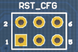
| + | This header added in V2. | ||
| + | |||
| + | [[Image:RST-CFG.png|none]] | ||
| + | |||
| + | Jumper on 4 and 6: JTAG1's RST (Pin 21) directly connected to target's RST pin. | ||
| + | One Jumper on 1 and 3, another jumper on 2 and 4: JTAG1's RST (pin 21) is connected to target's RST pin via a NPN transistor to reverse the polarity. | ||
| + | |||
| + | == SWD Enable Jumper == | ||
| + | |||
| + | This jumper is added in V2. | ||
| + | |||
| + | [[image:Swd-enable.png|none]] | ||
| + | |||
| + | Jumper on 1 and 2: Enable SWD header (which disables SPI1) | ||
| + | Jumper on 2 and 3: Disable SWD header (which enables SPI1) | ||
| + | |||
| + | == SWD Header == | ||
| + | |||
| + | This jumper is added in V2. | ||
| + | |||
| + | [[Image:Swd-header.png|none]] | ||
| + | |||
| + | The pinout is compatible with ST-Link. | ||
| + | |||
| + | {| | ||
| + | ! align="left"|Pin # | ||
| + | ! Description | ||
| + | |- | ||
| + | | 1 | ||
| + | | +3.3V | ||
| + | |- | ||
| + | | 2 | ||
| + | | SWDCLK | ||
| + | |- | ||
| + | | 3 | ||
| + | | GND | ||
| + | |- | ||
| + | | 4 | ||
| + | | SWDIO | ||
| + | |- | ||
| + | | 5 | ||
| + | | NRST | ||
| + | |- | ||
| + | | 6 | ||
| + | | SWO | ||
| + | |} | ||
| + | |||
| + | = Pin Connections = | ||
| + | |||
| + | {|class="wikitable" style="background:#cccc99;color:black;width:80%;" border="1" cellpadding="5" cellspacing="0" align="center" | ||
| + | | align="center" style="background:#f0f0f0;"|'''FT2232H''' | ||
| + | | align="center" style="background:#f0f0f0;"|'''20 PIN JTAG Header''' | ||
| + | | align="center" style="background:#f0f0f0;"|'''SPI Header 1''' | ||
| + | | align="center" style="background:#f0f0f0;"|'''DB9 Connector''' | ||
| + | | align="center" style="background:#f0f0f0;"|'''RS232 Level Output Header''' | ||
| + | | align="center" style="background:#f0f0f0;"|'''TTL Level Output Header''' | ||
| + | | align="center" style="background:#f0f0f0;"|'''SPI Header 2''' | ||
| + | | align="center" style="background:#f0f0f0;"|'''SWD Header (Added in V2)''' | ||
| + | | align="center" style="background:#f0f0f0;"|'''Memo''' | ||
| + | |- style="align=center;background:white; color:black" | ||
| + | | ADBUS0||TCK||SCK||||||||||SWDCLK|| | ||
| + | |- style="background:#f0f0f0; color:black" | ||
| + | | ADBUS1||TDI||MOSI||||||||||SWDIO|| | ||
| + | |- style="align=center;background:white; color:black" | ||
| + | | ADBUS2||TDO||MISO|||||||||||| | ||
| + | |- style="background:#f0f0f0; color:black" | ||
| + | | ADBUS3||TMS||CS|||||||||||| | ||
| + | |- style="align=center;background:white; color:black" | ||
| + | | ADBUS4||RST|||||||||||||| | ||
| + | |- style="background:#f0f0f0; color:black" | ||
| + | | ADBUS5||nTRST|||||||||||||| | ||
| + | |- style="align=center;background:white; color:black" | ||
| + | | ADBUS6||DBGRQ|||||||||||||| | ||
| + | |- style="background:#f0f0f0; color:black" | ||
| + | | ADBUS7||RTCK|||||||||||||| | ||
| + | |- style="align=center;background:white; color:black" | ||
| + | | |||||||||||||||| | ||
| + | |- style="background:#f0f0f0; color:black" | ||
| + | | ACBUS0||DBGACK|||||||||||||| | ||
| + | |- style="align=center;background:white; color:black" | ||
| + | | ACBUS1||||||||||||||||Connected to nTRST pin of JTAG Header, (input) | ||
| + | |- style="background:#f0f0f0; color:black" | ||
| + | | ACBUS2||||||||||||||NRST||Connected to RST pin of JTAG Header, as (input) | ||
| + | |- style="align=center;background:white; color:black" | ||
| + | | ACBUS3||||||||||||||||OEN Pin (enable buffer chip), active low (output) | ||
| + | |- style="background:#f0f0f0; color:black" | ||
| + | | ACBUS4||||||||||||||||Target present pin. Detect VTAR, active low (input) | ||
| + | |- style="align=center;background:white; color:black" | ||
| + | | ACBUS5|||||||||||||||| | ||
| + | |- style="background:#f0f0f0; color:black" | ||
| + | | ACBUS6|||||||||||||||| | ||
| + | |- style="align=center;background:white; color:black" | ||
| + | | ACBUS7|||||||||||||||| | ||
| + | |- style="background:#f0f0f0; color:black" | ||
| + | | |||||||||||||||| | ||
| + | |- style="align=center;background:white; color:black" | ||
| + | | BDBUS0||||||TX||TX||TX||SCK|||| | ||
| + | |- style="background:#f0f0f0; color:black" | ||
| + | | BDBUS1||||||RX||RX||RX||MOSI||SWO|| | ||
| + | |- style="align=center;background:white; color:black" | ||
| + | | BDBUS2||||||RTS||RTS||RTS||MISO|||| | ||
| + | |- style="background:#f0f0f0; color:black" | ||
| + | | BDBUS3||||||CTS||CTS||CTS||CS|||| | ||
| + | |- style="align=center;background:white; color:black" | ||
| + | | BDBUS4||||||DTR||DTR||DTR|||||| | ||
| + | |- style="background:#f0f0f0; color:black" | ||
| + | | BDBUS5||||||DSR||DSR||DSR|||||| | ||
| + | |- style="align=center;background:white; color:black" | ||
| + | | BDBUS6||||||DCD||DCD||DCD|||||| | ||
| + | |- style="background:#f0f0f0; color:black" | ||
| + | | BDBUS7||||||RI||RI||RI|||||| | ||
| + | |- style="align=center;background:white; color:black" | ||
| + | | |||||||||||||||| | ||
| + | |- style="background:#f0f0f0; color:black" | ||
| + | | BCBUS0|||||||||||||||| | ||
| + | |- style="align=center;background:white; color:black" | ||
| + | | BCBUS1|||||||||||||||| | ||
| + | |- style="background:#f0f0f0; color:black" | ||
| + | | BCBUS2|||||||||||||||| | ||
| + | |- style="align=center;background:white; color:black" | ||
| + | | BCBUS3||||||||||||||||RX LED | ||
| + | |- style="background:#f0f0f0; color:black" | ||
| + | | BCBUS4||||||||||||||||TX LED | ||
| + | |- style="align=center;background:white; color:black" | ||
| + | | BCBUS5|||||||||||||||| | ||
| + | |- style="background:#f0f0f0; color:black" | ||
| + | | BCBUS6|||||||||||||||| | ||
| + | |- style="align=center;background:white; color:black" | ||
| + | | BCBUS7|||||||||||||||| | ||
| + | |- style="background:#f0f0f0; color:black" | ||
| + | | |||||||||||||||| | ||
| + | |- style="align=center;background:white; color:black" | ||
| + | | <span style="text-decoration: overline">PWREN</span>||||||||||||||||Enable MAX3243. Active low (output) | ||
| + | |} | ||
| + | |||
| + | <span class="plainlinks"> | ||
| + | |||
| + | <include nopre noesc src="/home/tiao/public_html/tiaowiki/wiki/extensions/include/jtag.inc"/> | ||
| + | |||
| + | Buy various JTAG cables for your Satellite Receiver, Cable Modem, Wireless Router, Standard Wiggler from [http://www.easymg.com http://www.easymg.com] and [http://www.diygadget.com http://www.diygadget.com] | ||
| + | </span> | ||
Latest revision as of 21:08, 3 November 2017
Contents
- 1 Overview
- 2 Technical Specifications
- 3 Board Dimensions
- 4 Board Layout
- 5 Connector Pinout & LEDs
- 5.1 DB9 Male RS232
- 5.2 SPI Connector 1
- 5.3 RS232 Level 2.54mm IDC Header
- 5.4 20 PIN JTAG Connector
- 5.5 MAX3243 Auto Power Down Jumper
- 5.6 Buffer Enable Jumper
- 5.7 Buffer Chip Power Selection Jumper
- 5.8 Serial RS232/TTL level Selection Jumper
- 5.9 TTL Level Serial Connector
- 5.10 SPI Connector 2
- 5.11 PWR/RX/TX LEDs
- 5.12 Target Board Power LED
- 5.13 RST signal polarity select
- 5.14 SWD Enable Jumper
- 5.15 SWD Header
- 6 Pin Connections
Buy various JTAG cables for your Satellite Receiver, Cable Modem, Wireless Router, Standard Wiggler from http://www.easymg.com and http://www.diygadget.com
Overview
The TIAO USB Multi Protocol Adapter (TUMPA) is a multi-functional USB communication adapter for hobbyists or engineers. The adapter is based on FDTI's flagship communication chip FT2232H, a USB 2.0 Hi-Speed (480Mb/s) to UART/FIFO IC. It has two multi-protocol synchronous serial engines (MPSSEs) which allow for communication using JTAG, I2C and SPI on two channels simultaneously.
Looking for PDF version of this manual? It is here:
Download PDF version of this manual
Thanks to stealther for creating the PDF manual.
Technical Specifications
- SWD support (Added in V2)
- RST line jumper header (added in V2)
- USB 2.0 Hi-Speed (480Mb/s)
- JTAG / IEEE 1149.1 compatible.
- JTAG Baudrate up to 30Mbits/sec (programmable)
- On board voltage translation via 74LVC14T245 (can be enabled / disabled via software or jumper)
- JTAG signals are 5V to 1.8V tolerant
- ARM Muli-ICE 20-pin header compatible.
- Separate SPI/I2C/Serial interfaces
- Configurable output of RS232 (MAX3243) or TTL level for serial communication
- Configurable auto power down for MAX3243
- Target board can be powered by TUMPA (3.3V) or self powered (via jumper)
- 4 on-board LEDs / PWR, Targt PWR, TX and RX
- 1 2x10 20 PIN JTAG header
- 1 2x5 10 PIN RS232 level 2.54mm IDC header
- 1 2x6 10 PIN TTL level 2.54mm IDC header
- 2 2x3 6 PIN SPI 2.54mm IDC header
- 1 x DB9 connector (male, RS232 level)
- Target board power jumper
- Buffer chip enable jumper
- RS232 chip auto power down jumper
- RS232 or TTL output jumber
- USB Hot-Plug / JTAG Hot-Plug.
- USB over-current protection via on-board resetable fuse.
- Strong ESD protection on USB signals.
- Based on the FTDI FT2232H USB device.
- Designed for FTDI MPSSE easy-to-use.
- Free drivers for Linux.
- Free drivers for Windows XP, Windows Vista and Windows 7
- Support both 32 bit and 64 bit operating systems
- Board dimension: 65.41mm X 58.55mm (2.58" X 2.31")
Board Dimensions
V1:
V2:
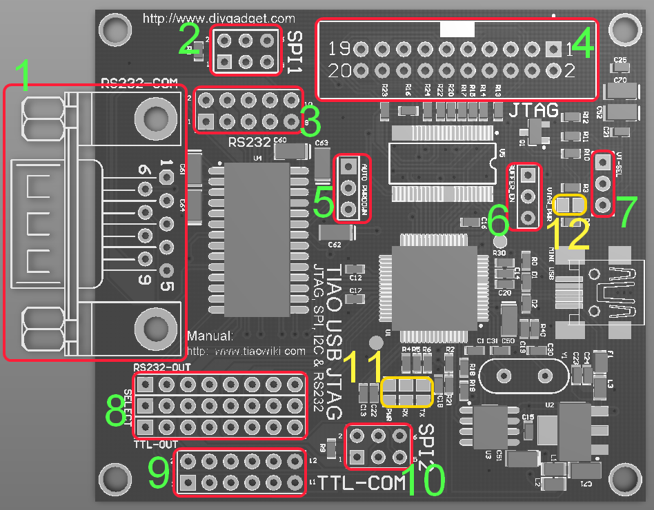
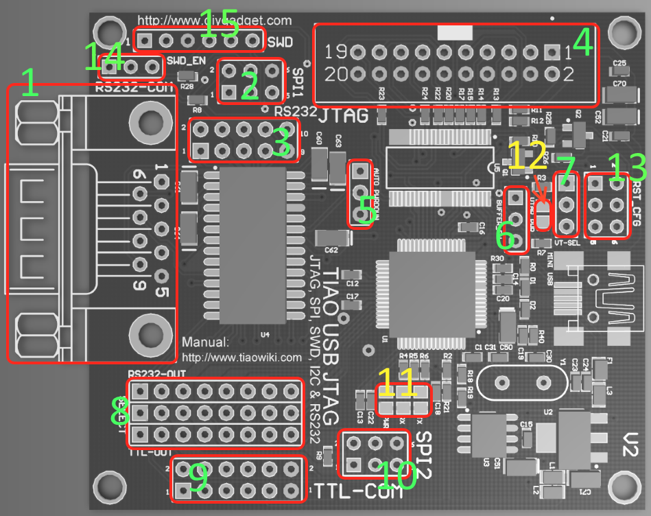
Board Layout
V1:
V2:
- DB9 male RS232 connector (Channel B)
- 2x3 standard 6 PIN 2.54mm IDC SPI connector (Channel A)
- RS232 Level 2.54mm IDC Header
- 2x10 standard 20 PIN 2.54mm IDC JTAG connector (Channel A)
- Auto power down jumper header for MAX3243 (force on or auto power down). Default force on (jumper is on pin 1and 2)
- Buffer enable jumper header for 74LVC16T245. Default is always enabled. (jumper on pin 2 and 3)
- Buffer chip 74LVC16T245 Vcc(B) power select jumper. Default is to power Vcc(B) by TUMPA (3.3V only) (jumper on pin 1 and 2)
- 3x8 PIN RS232 or TTL level serial communication jumpmer. Default is RS232 output (jumpers short top row and middle rows) (Channel B)
- 2x6 PIN TTL level 2.54mm IDC serial header (channel B)
- 2x3 PIN 2.54mm IDC SPI header (channel B)
- Status LEDs. From left to right: Power (indicates TUMPA is powered on), RX and TX
- Target board power LED. Indicates target board has power
- RST signal polarity select. Change the RST signal polarity
- SWD Enable Jumper. Enable or disable SWD
- SWD header. Header for SWD
Connector Pinout & LEDs
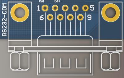
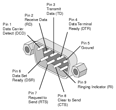
DB9 Male RS232
This connector is enabled only if RS232/TTL jumpers are on RS232-OUT, see Serial RS232/TTL level Selection Jumper
| Pin # | Acronym | Full name | Direction | Description |
|---|---|---|---|---|
| 1 | DCD | Data Carrier Detect | <<-- | Modem connected to another |
| 2 | RxD | Receive Data | <<-- | Receives bytes into PC |
| 3 | TxD | Transmit Data | -->> | Transmits bytes out of PC |
| 4 | DTR | Data Terminal Ready | -->> | I'm ready to communicate |
| 5 | SG | Signal Ground | Ground/GND | |
| 6 | DSR | Data Set Ready | <<-- | I'm ready to communicate |
| 7 | RTS | Request To Send | -->> | RTS/CTS flow control |
| 8 | CTS | Clear To Send | <<-- | RTS/CTS flow control |
| 9 | RI | Ring Indicator | <<-- | Telephone Line Ringing |
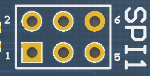
SPI Connector 1
| Pin # | Description |
|---|---|
| 1 | MISO |
| 2 | Vcc (connected to on board 3.3V) |
| 3 | SCK |
| 4 | MOSI |
| 5 | CS |
| 6 | GND |
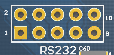
RS232 Level 2.54mm IDC Header
This connector is enabled only if RS232/TTL jumpers are on RS232-OUT, see Serial RS232/TTL level Selection Jumper
For your convenience, we added this header. This header is inter connected to the DB9 connector. The pinout is different then the pinout of DB 9 connector, however the extra pin (PIN 10) is connected to on board 3.3V power. GND pin (PIN 9) and +3.3V PIN (PIN 10) are always enabled regardless the jumpers position of Serial RS232/TTL level Selection Jumper.
This is the pinout of the RS232 level 2.54mm IDC header:
| Pin # | Description |
|---|---|
| 1 | RI |
| 2 | DCD |
| 3 | DSR |
| 4 | CTS |
| 5 | RX |
| 6 | TX |
| 7 | RTS |
| 8 | DTR |
| 9 | GND |
| 10 | +3.3V |
20 PIN JTAG Connector
| Pin # | Description |
|---|---|
| 1 | VTAR |
| 3 | nTRST |
| 5 | TDI |
| 7 | TMS |
| 9 | TCK |
| 11 | RTCK |
| 13 | TDO |
| 15 | RST |
| 17 | DBGRQ |
| 19 | DBGACK |
| 2 | Not Connected |
| 4, 6, 8, 10, 12, 14, 16, 18, 20 | GND |
MAX3243 Auto Power Down Jumper
This jumper controls whether to always enable MAX3243 or let FT2232H automatically enables it (save power).
- Jumper on PIN 1 and PIN 2: Always enable MAX3243
- Jumper on PIN 2 and PIN 3: FT2232H (PWREN, PIN 60)controls when to enable or disable MAX3243.
Buffer Enable Jumper
This jumper controls whether to software enable/disable buffer chip (74LVC16T254).
- Jumper on PIN 1 and PIN 2: Enable (Low)/Disable (High) 74LVC16T245 via FT2232H's ACBUS3 (PIN 29).
- Jumper on PIN 2 and PIN 3: Always enable 74LVC16T245
Buffer Chip Power Selection Jumper
This jumper controls how to power the buffer / voltage translator chip (74LVC16T245)
The 74LVC16T245's Vcc(A) is connected to on board +3.3V. You can either power the Vcc(B) using on board +3.3V or powered by the target board. If powered by target board, please make sure the target board's power is in the range of +1.8V - +5.5V.
- Jumper on PIN 1 and PIN 2: Power the buffer chip 74LVC16T245's Vcc(B) via the on board +3.3V source.
- Jumper on PIN 2 and PIN 3: Power the buffer chio 74LVC16T245's Vcc(B) by target board. (PIN 3 of this header is connected to JTAG header's PIN 1)
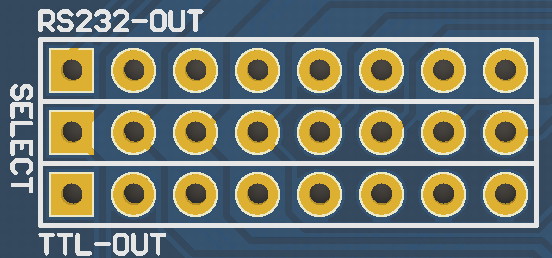
Serial RS232/TTL level Selection Jumper
These jumpers allows you to have serial communication at either RS232 level or TTL level.
- Jumpers short top row (RS232-OUT) and middle row (SELECT) (this is the default): enable RS232 level serial output. (thus DB9 Connector and RS232 Level 2.54mm IDC Header are enabled)
- Jumpers short middle row (SELECT)and bottom row (TTL-OUT): enable TTL level serial output. (thus TTL Level Serial Connectoris enabled)
TTL Level Serial Connector
This connector is enabled only if RS232/TTL jumpers are on TTL-OUT, see Serial RS232/TTL level Selection Jumper
| Pin # | Description |
|---|---|
| 1 | Tx |
| 2 | Rx |
| 3 | RTS |
| 4 | CTS |
| 5 | DTR |
| 6 | DSR |
| 7 | DCD |
| 8 | RI |
| 9 | +3.3V |
| 10 | +5V (USB Power) |
| 11, 12 | GND |
The power pins (9, 10, 11 and 12) are always connected, regardless of the jumper positions of Serial RS232/TTL level Selection Jumper.
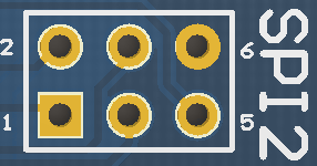
SPI Connector 2
| Pin # | Description |
|---|---|
| 1 | MISO |
| 2 | Vcc (connected to on board 3.3V) |
| 3 | SCK |
| 4 | MOSI |
| 5 | CS |
| 6 | GND |
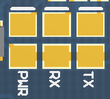
PWR/RX/TX LEDs
- PWR: indicates the TUMPA board is connected to USB port of the computer and on board voltage regulator outputs +3.3V.
- RX: Indicates FT2232H is receiving bytes from target via serial communication channel B
- TX: Indicates FT2232H is transmitting bytes to target via serial communication channel B
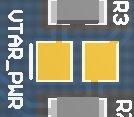
Target Board Power LED
- LED is ON: Target board (PIN 1 of JTAG Header) has power supply > 3.3V.
- LED is OFF: Target board (PIN 1 of JTAG Header) has power supply < 3.3V or no power.
The VTAR can also be detected by software. If VTAR has voltage > 3.3V, ACBUS4 (PIN 30) of FT2232H will be LOW. Otherwise it will be HIGH.
RST signal polarity select
This header added in V2.
Jumper on 4 and 6: JTAG1's RST (Pin 21) directly connected to target's RST pin. One Jumper on 1 and 3, another jumper on 2 and 4: JTAG1's RST (pin 21) is connected to target's RST pin via a NPN transistor to reverse the polarity.
SWD Enable Jumper
This jumper is added in V2.
Jumper on 1 and 2: Enable SWD header (which disables SPI1) Jumper on 2 and 3: Disable SWD header (which enables SPI1)
SWD Header
This jumper is added in V2.
The pinout is compatible with ST-Link.
| Pin # | Description |
|---|---|
| 1 | +3.3V |
| 2 | SWDCLK |
| 3 | GND |
| 4 | SWDIO |
| 5 | NRST |
| 6 | SWO |
Pin Connections
| FT2232H | 20 PIN JTAG Header | SPI Header 1 | DB9 Connector | RS232 Level Output Header | TTL Level Output Header | SPI Header 2 | SWD Header (Added in V2) | Memo |
| ADBUS0 | TCK | SCK | SWDCLK | |||||
| ADBUS1 | TDI | MOSI | SWDIO | |||||
| ADBUS2 | TDO | MISO | ||||||
| ADBUS3 | TMS | CS | ||||||
| ADBUS4 | RST | |||||||
| ADBUS5 | nTRST | |||||||
| ADBUS6 | DBGRQ | |||||||
| ADBUS7 | RTCK | |||||||
| ACBUS0 | DBGACK | |||||||
| ACBUS1 | Connected to nTRST pin of JTAG Header, (input) | |||||||
| ACBUS2 | NRST | Connected to RST pin of JTAG Header, as (input) | ||||||
| ACBUS3 | OEN Pin (enable buffer chip), active low (output) | |||||||
| ACBUS4 | Target present pin. Detect VTAR, active low (input) | |||||||
| ACBUS5 | ||||||||
| ACBUS6 | ||||||||
| ACBUS7 | ||||||||
| BDBUS0 | TX | TX | TX | SCK | ||||
| BDBUS1 | RX | RX | RX | MOSI | SWO | |||
| BDBUS2 | RTS | RTS | RTS | MISO | ||||
| BDBUS3 | CTS | CTS | CTS | CS | ||||
| BDBUS4 | DTR | DTR | DTR | |||||
| BDBUS5 | DSR | DSR | DSR | |||||
| BDBUS6 | DCD | DCD | DCD | |||||
| BDBUS7 | RI | RI | RI | |||||
| BCBUS0 | ||||||||
| BCBUS1 | ||||||||
| BCBUS2 | ||||||||
| BCBUS3 | RX LED | |||||||
| BCBUS4 | TX LED | |||||||
| BCBUS5 | ||||||||
| BCBUS6 | ||||||||
| BCBUS7 | ||||||||
| PWREN | Enable MAX3243. Active low (output) |
Buy various JTAG cables for your Satellite Receiver, Cable Modem, Wireless Router, Standard Wiggler from http://www.easymg.com and http://www.diygadget.com

10 PCS, 10cm x 10cm, 2 layers prototype for $38.80 shipped!
